New Chiplet Interconnect Specifications now available to all for an Extensible Link Layer (LL 1.0) and PHY Layer (BoW 2.0)
April 19th, 2023 – Today, the Open Compute Project Foundation (OCP), the nonprofit organization bringing hyperscale innovations to all, announces it has taken important steps in establishing an open Chiplet economy with the release of a new open-to-all Chiplet interconnect link layer specification and an evolution of its previously-released Bunch of Wires (BoW) PHY specification. The link layer uniquely defines profiles that allow customization of the mapping from transport layer services to underlying PHY via link layer services, allowing choice of PHY without affecting other layers. BoW 2.0 builds on hundreds of millions of investment dollars in BoW 1.0 by doubling speed and maintaining backwards compatibility.
 “The OCP recognized several years ago that innovation in silicon needed to be amplified, just as the constraints of larger silicon dies were beginning to impede progress. The OCP created its vision for an open Chiplet economy with the intent of being a catalyst for change by establishing a strong community to deliver on the new standardizations, tools and best practices around technical and business workflows that would be required for a truly open economy, where vendors would sell Chiplets embodying their IP to integrators that would build specialized System in Package (SiP)s. Moving forward the OCP intends to become the front door to an open Chiplet marketplace, providing standardizations allowing Chiplet vendors to self-certify, or 3rd party organizations to independently verify, Chiplet Known Good Die (KGD) characteristics," said Cliff Grossner Ph.D., VP Market Intelligence and Innovation at the Open Compute Project Foundation.
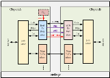
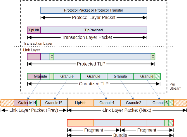
The development of the OCP ODSA (Open Domain-Specific Architecture) Link Layer specification is focused on the silicon die disaggregation use case maintaining simplicity to serve as many markets as possible, with key features, such as: (1) extensibility defining interface profiles allowing the addition of new link layer features, customization to bus protocols and enabling Chiplet interconnect interoperability, (2) portability across different die implementation methodologies and process nodes, (3) ability to scale with support for multiple PHY slices and different data rates, (4) while keeping latency low, especially with use of Forward Error Correction (FEC) eliminating where possible serialization due to Cyclic Redundancy Check (CRC).
Staying true to its non-prescriptive philosophy allowing the SiP builder as many degrees of freedom as possible to meet the needs of specific markets, BoW 2.0 includes significant advancements on top of doubling top speed to 512 Gb/s per 16 lane slice, including: (1) new energy efficient operations with gated clock and data line inactive modes that can save up to 90% of power consumed for interconnect, (2) half-width slices for dies with smaller absolute beachfront requirements, (3) sideband slices for channel management, (4) bidirectional slices with direction configurable across channel, and (5) and bump redundancy for improved reliability on failure.
"Specialization using Chiplet technology is one very promising approach to getting scientifically relevant specializations into future supercomputers at an affordable cost. Creating efficient open standards for the inter-die communication between the Chiplets is an essential underpinning for this approach,” said John Shalf, Department Head for Computer Science at Lawrence Berkeley Laboratory.
“We can see the first visible seedlings of the open Chiplet economy sprout with the release of LL 1.0 and BoW 2.0 complementing the recent release of CDXML and establishing an alliance with JEDEC and work on standardized Chiplet test benches and interconnect benchmarks. We are at an inflection point where Chiplet vendors have a fairly complete set of standards and tools available to derisk building Chiplet product sets. The market leaders developing Chiplets are still playing a very important role filling gaps that they identify in current standards and we expect to see these additional learnings materialize as updates to existing standards as the open Chiplet economy matures,” said Bapi Vinnakota Ph.D., ODSA Project lead at OCP.
“The silicon supply chain requires diversity to serve many vertical electronic equipment segments including automotive, personal data processing, data center and enterprise data processing, communications infrastructure, medical, defense, aerospace and industrial. Each market includes application-specific requirements that make it unlikely that any one supplier has the broad expertise to serve all these markets. A diverse Chiplet supply chain will emerge supporting many players and lowering the barrier to entry. This will enable rapid innovation. Open communities sharing the effort for building common tools, prototypes, business workflows and standardizations are critical to accelerate a Chiplet Economy,” said Tom Hackenberg, Principal Analyst, Computing & Software Semiconductor, Memory and Computing Division, Yole Group.
Support from Key Stakeholders
ADI
“The additional features of BoW 2.0 position it as an attractive D2D interface due to its flexibility and large bandwidth scalability. They make BoW 2.0 interesting for both lower performance systems with low-cost packaging as well as high performance applications where advanced packaging and redundancy is a must,” said Susan Feindt, Fellow, Director of Physical Technology Strategy, Analog Devices.
Applied Materials
“As traditional Moore’s Law scaling slows and becomes more expensive, new design and manufacturing paradigms are being adopted by chipmakers and systems companies to advance their PPACt™ roadmaps. Chiplet Interconnects and advanced packaging solutions are an integral part of the IEEE Heterogeneous Integration Roadmap. The availability of BOW 2.0 as an open standard will enable high performance, power efficient integration of Chiplets, and Applied Materials’ suite of equipment enables a range of advanced packaging solutions,” said Subi Kengeri, Vice President, AI Systems Solutions at Applied Materials.
NXP
"NXP® strongly supports standards that welcome a broad and inclusive global ecosystem of partners. ODSA BoW 2.0 is a great example of a chiplet PHY specification that couples to a minimalistic, low-latency link layer to enable flexible die disaggregation and bus protocol integration. We are actively developing a BoW PHY design to validate and demonstrate readiness for future cost-effective and disruptive multi-chip products in the automotive and secure connected edge processing space," explains Mike Leary, vice president of engineering at NXP Semiconductors.
Tessolve
“Tessolve is a semiconductor services company, supporting our clients to create embedded products. We therefore continuously strive to ensure our expertise and services stay ahead of the expected market demands. Tessolve was thus an early member of OCP’s ODSA Project given its leadership in the drive to standardize the adoption of Chiplets and has been active in the various committees. Specifically, Tessolve has designed boards to connect the first BoW-based silicon chips to be manufactured. Tessolve is also working with clients to advise on test strategies both at the Chiplet and system level, to ensure both high test coverage and sufficient final yield. Tessolve is also involved in the drive to develop an independent compliance test to better ensure integration of Chiplets,” said Dr. Mike Bartley, SVP VLSI, Tessolve.
Blue Cheetah Analog Design
"The flexibility and interoperability fostered by the ODSA BoW 2.0 PHY and link layer specifications are critical enablers for a broad range of disaggregated die SiPs for applications spanning low-cost consumer electronics, mobile devices, and high-end datacenter/AI systems. Blue Cheetah's state-of-the-art BoW-based solutions have already been adopted by multiple customers spanning all of these application categories, and we look forward to continuing to work with the OCP ODSA Project and our partners to advance the Chiplet revolution," said Elad Alon, CEO of Blue Cheetah.
d-Matrix.ai
“The BoW 2.0 interconnect specification will enable more efficient AI inference by doubling the speed of inter-die communication, helping to create Chiplet solutions that efficiently scale from the largest datacenter all the way to a developer’s desktop,” said Sid Sheth, CEO and Founder of d-Matrix. “The OCP continues to promote best practices and robust standards that are driving industry innovation and creating new opportunities for companies in the field of AI.”
DreamBig Semiconductor
“DreamBig has taped out its first Chiplet Hub in TSMC 5nm using BCA(Blue Cheetah) BoW PHY with multiple ecosystem partners taping out other BoW based Chiplets (Like DDR4/DDR5/HBM3 Controllers, Accelerators, Processors etc.) in the span of next 6 months. This will be the inception of Commercial Chiplet MarketPlace (CCMP) where DreamBig will be leading by providing the ODSA-compliant BoW-based Chiplet Hub with inherent support for Memory, Ethernet, CXL-based Subsystem. We look forward to working with the OCP ODSA Project to expand the reach and impact of CCMP, enabling greater innovation and growth in the Chiplet ecosystem,” said Sohail Syed, CEO of DreamBig Semiconductor.
VeriSilicon Microelectronics
“We see a vision of the future where silicon products all leverage a vibrant ecosystem of Chiplets. Clearly defined Chiplet interoperability and communication will create an industry-wide library of IP-as-a-Chiplet functionality that accelerates both innovation and time-to-market. With the OCP ODSA Project enabling this vision using proven BoW technology, the industry takes a leap forward into this new reality,” said Martyn Humphries, Senior VP, Advanced Technology Platform Group, VeriSilicon Microelectronics.
APEX Semiconductor
"Apex semiconductors is an early contributor to the BoW specification and has been a strong supporter of this technology. We have developed the industry's first three Chiplet SmartNIC platform composed of a CXL I/O hub and two 16-core RISC-V processors, for our ecosystem partners, using Blue Cheetah's BoW D2D PHY. The BoW D2D interconnect standard is a key enabler for this game-changing solution which is scalable and extensible," said Suresh Subramaniam, System and Packaging Lead at Apex Semiconductor.
About the Open Compute Project Foundation
At the core of the open compute project (OCP) is its community of hyperscale data center operators, joined by telecom and colocation providers and enterprise IT users, working with vendors to develop open innovations that when embedded in products are deployed from the cloud to the edge. The OCP Foundation is responsible for fostering and serving the OCP community to meet the market and shape the future, taking hyperscale led innovations to everyone. Meeting the market is accomplished through open designs and best practices, and with data center facility and IT equipment embedding OCP community developed innovations for efficiency, at-scale operations, and sustainability. Shaping the future includes investing in strategic initiatives that prepare the IT ecosystem for major changes, such as AI & ML, optics, advanced cooling techniques, and composable silicon. Learn more at www.opencompute.org.
# # #
Media Contact
Dirk Van Slyke
Open Compute Project Foundation
Vice President, Chief Marketing Officer
dirkv@opencompute.org
Mobile: +1 303-999-7398