Introduction
Chiplet-based products have recently emerged across multiple industry-leading semiconductor vendors and cloud providers, including AMD, Intel, Broadcom, Amazon and Ampere, as a potential technology to extend Moore’s law. Their remarkable growth has been driven by a mixture of motivations: (1) to avoid very large die sizes for improved yields; (2) to enable product diversification through mix-and-match strategies for reuse and cost savings, and (3) to promote heterogeneous integration - integrating chiplets from multiple process nodes for function, cost and/or performance optimization. One expects these motivations are equally relevant to all companies developing semiconductor products. As an example, only 60% or less of the logic in domain-specific accelerators is actually domain specific. Companies could, in theory, buy IP in the form of chiplets, to reduce both their costs and time-to-market. In practice, technical and business challenges have largely restricted the development of chiplet-based designs to organizations with the financial resources to control the entire development stack for their product.
The intricacies of designing and manufacturing chiplet-based products are multifaceted and complex, driven by the simple fact that a chiplet-based product consists of multiple silicon die(chiplets), integrated into one package. First, these chiplets need to communicate with one another, necessitating a physical and logical interconnection network within the package. Second, relative to monolithic silicon IC design, chiplet design requires integration across the value chain. Product designers now have to consider the impact of factors, such as packaging, assembly and test technologies, traditionally addressed at the “backend” of the SoC production cycle for all but the most complex products. Last, the manufacturing workflow becomes more complex, encompassing tasks such as inventory management of chiplets, more advanced packaging technology, an interplay between test and packaging (for example, choosing to package expensive chiplets last to reduce spoilage costs). When expanded to integrating chiplets from multiple vendors, more factors add complexity including business contracts around known good die, where inventory should be physically stored and for how long, and full product quality ownership.
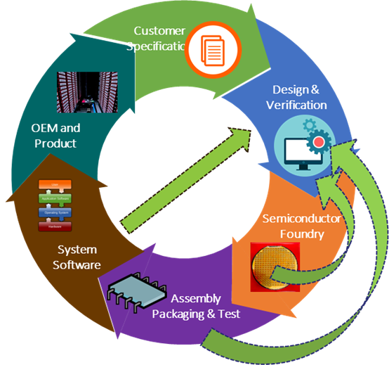
Figure 1: Chiplets require integration across the semiconductor value chain
A Framework for Diverse Open Efforts is Required
Industry analysts at Yole Group research estimate that the market for chiplets may grow to $180 Billion by 2027. Such a large market is likely only possible if chiplets are used everywhere chips are. Analysts from Accenture segment silicon IC consumption across five primary markets in order of size: Data Processing (40%), Communication (30%), Automotive, Consumer devices and Industrial (each about 10%). As with other applications for software and hardware, open standards and activities can accelerate the development and growth of robust multi-vendor chiplet supply chains with lots of choice for the end user to create the customizations they desire. It is worth noting that product performance power and cost requirements vary by three orders of magnitude across these markets. It is unlikely a single set of deeply prescriptive standards can serve the entire universe of potential chiplet applications.
In developing an open framework, we believe there is a lot to be learned from open community efforts in software. Linux is an example of an open-source effort that serves diverse applications. Its core is a community-developed kernel that can freely be adapted by any individual or entity without restriction. The market has developed multiple flavors of application-specific Linux, each serving broad segments, many of which are incompatible with one another. Unrestricted access and market-led adaptability has led to unstoppable growth with Linux becoming the dominant OS for virtually every application.
An Open Chiplet Economy
The Open Compute Project (OCP) believes that, as with Linux, the right open framework for chiplets, is to create a core set of adaptable standards and tools that facilitate chiplet-based product design and manufacturing. The open chiplet economy will be most productive, not by imposing inflexible standards, but rather by focusing on continually reducing the development and manufacturing friction in heterogeneous integration for chiplet-based products across multiple vendors, process nodes, packaging technologies, applications etc. This can be achieved by creating standards and open tools in three areas:
- Die-to-die interfaces: this includes creating layered protocols for die-to-die communication, open channel models for interface design, example open package designs, etc.
- Design and manufacturing workflows - addressing problems in digital descriptions of chiplets for EDA toolflows, reference design flows, modularity in packaging and assembly, chiplet testing, electronic data sheets, architecture exploration tools, etc.
- Business workflows - addressing problems in business contracts for known good die, cost models for chiplet-based products, creating catalogs of chiplets, and an open marketplace where chiplet suppliers can showcase their wares.
Open Compute Project Activities in the Open Chiplet Economy
Effective support and development for the Open Chiplet Economy requires cooperation across several standards organizations including the OCP, the IEEE, the UCIe consortium, SEMI, IMAPS and other organizations. This section focuses on the activities of the Open Domain-Specific Architecture (ODSA) Project within the OCP to be a catalyst for enabling an open chiplet economy. The ODSA Project includes volunteers from over fifty companies that participate across six work efforts and have delivered significant open specifications and reference material. Some examples are as follows:
- A Die-to-Die Interface Stack. The ODSA specified the only open die-to-die interface to fully support heterogeneous integration and allow easy customization across a wide range of performance and cost points for chiplets - with industry implementations from mature 65nm nodes to 5nm nodes, a realized power dissipation less than 0.3 pJ/bit and an edge bandwidth greater than 1 Tbps/mm in commodity packaging to far higher performance in advanced packaging technologies, spanning line rates ranging from IoT to hyperscaler data center accelerators (BoW 1.0, BoW 2.0, TLP, DiPort).
- A specification language for EDA Workflows: The chiplet design exchange work effort of the ODSA has developed the first open language, CDXML, to describe chiplets. Standards to use CDXML are being developed cooperatively with JEDEC.The CDXML standard will enable electronic descriptions of chiplets for EDA and architecture workflows and will eventually be used by every commercial chiplet produced.
- Tools widely referenced as industry standards - a D2D PHY comparison spreadsheet used by designers to select the best D2D interconnect best for their product; a cost model for chiplet development; the first open chiplet package effort in the industry with corresponding open signal and power integrity analysis to guide other designers, and open test bench boards, allowing integration of chiplets that support the ODSA stack from multiple vendors, workshops, white papers and refereed conference papers on chiplet workflows and technology.
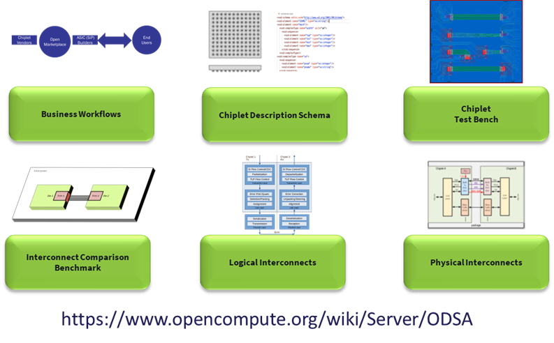
Figure 2: Open Domain-Specific Architecture project work efforts
The Status of the Open Chiplet Economy
Today, the Open Chiplet Economy has successfully transcended its conceptual stage. This transformation is evident in the existence of actual products and prototypes, encompassing chiplets, open development platforms, workflow tools, and interface intellectual property. For example, the ODSA stack has garnered substantial investment across several companies, totaling several hundred million dollars (examples in Figure 3). This investment has been channeled across diverse applications, including artificial intelligence, data centers and the Internet of Things (IoT). Vendors have recently announced test silicon for the UCIe interface. This concrete progress underscores the real-world applicability and potential wide scale impact of the Open Chiplet Economy.
| d-Matrix, TSMC 6nm, AI Product | 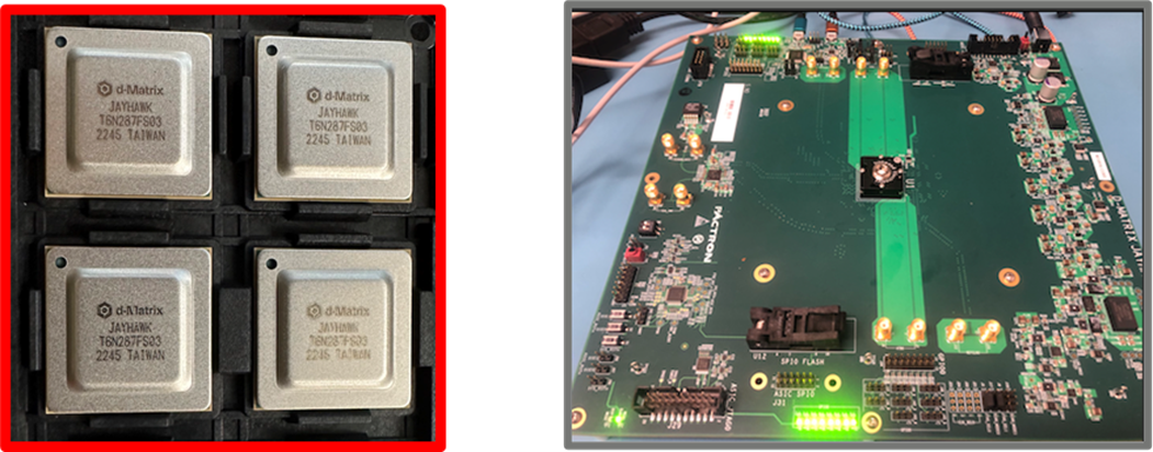 |
| Blue Cheetah Analog TSMC 12nm, IP Test Chip | 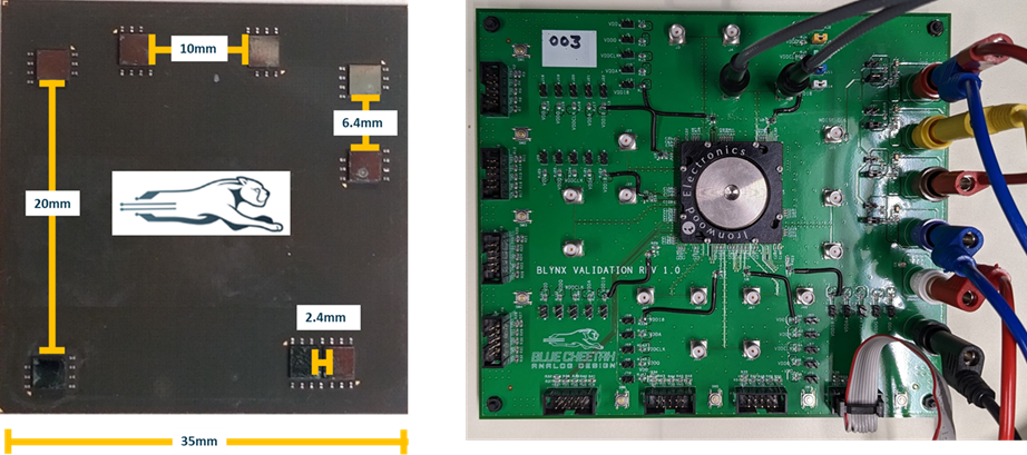 |
Figure 3: Silicon implementations of the BoW 1.0 protocol in an AI Product and IP Test Chip
Table 1 summarizes significant challenges and OCP/ODSA activities in this space. The OCP/ODSA will continue the expansion of activities to further diminish barriers to chiplets as follows:
- Expand the open test package to a suite of tools and platforms to accelerate the development of prototypes
- Use modular reference architectures along with associated workflows, to reduce packaging and assembly costs and development time, with a focus on enabling rapid prototyping.
- Establish an Open Chiplet Marketplace to both aid designers in identifying suitable chiplets for their projects, and provide an environment to chiplet vendors of all sizes to showcase their wares
Please join OCP/ODSA workstreams and spur innovation by contributing to the growth of a robust multi-vendor supply chain that reduces the time and cost to build and market chiplets and chiplet-based products. Through these multifaceted efforts, the Open Chiplet Economy is set to redefine the landscape of chiplet-based products and catalyze innovation in the field.
| Business Workflow | Chiplet Product Manufacturing | Chiplet Product Design | Chiplet Interconnect | |
| Standards |
Business catalog Known-Good Die contracts |
Digital Chiplet Physical Descriptions CDXML Modular Architecture |
Digital Chiplet Functional Descriptions |
|
| Tools and Reference |
SiP cost models Reuse business case Marketplace |
Package Analysis & Tools Device Test |
Architecgure Exploration PHY Selector |
Selection Guides Channel models |
| Production Support | Business Logistics | In-field management | Chiplet Catalog |
Table 1: Challenges and OCP/ODSA activities (in bold) in the Open Chiplet Economy
In the immediate future, you can engage in the latest developments at the upcoming 2023 OCP Global Summit, taking place October 17 to 19 in San Jose, CA. There are two relevant tracks dealing with Chiplets:
- The Server Breakout sessions: The Open Chiplet Economy takes place all afternoon of Thursday October 19 in 210BF of the SJCC Concourse Level.
- The first ever Open Chiplet Economy experience on the exhibit floor with products and prototypes in chiplets, IP and workflows from eleven companies.
- As part of the Future Technologies Symposium, Advanced package technologies for chiplet adoption and memory integration in HPC/AI applications. Wed, October 18, 12:55pm - 1:10pm | SJCC - Lower Level - LL20BC
See the full schedule and register here: https://www.opencompute.org/summit/global-summit