Chiplets
Read the latest news and updates from the Open Compute Project.
Browse 58 news articles
-
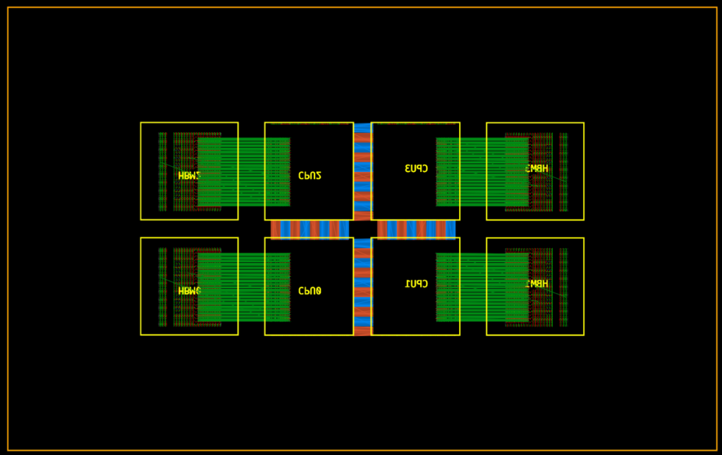
Thrace Systems – DankaChiplet(TM) Platform for 3D-IC Architects
Design your next 3D-IC with DankaChiplet(TM) Platform. Built on industry standards, such as IEEE2416 and CDXML, DankaChiplet enables you to quickly architect your next 3D-IC by exploring power analysis, bump planing, and substrate and interposer connectivity… -
Caliptra 1.0
This is version 1.0 of Caliptra which consists of IP and firmware for an integrated Root of Trust block. Caliptra targets datacenter-class SoCs like CPUs, GPUs, DPUs, TPUs. It is the specification, silicon logic, ROM and firmware… -
-
Caliptra R1
Caliptra consists of IP and firmware for an integrated Root of Trust block. Caliptra targets datacenter-class SoCs like CPUs, GPUs, DPUs, TPUs. It is the specification, silicon logic, ROM and firmware for implementing a Root of Trust… -
-
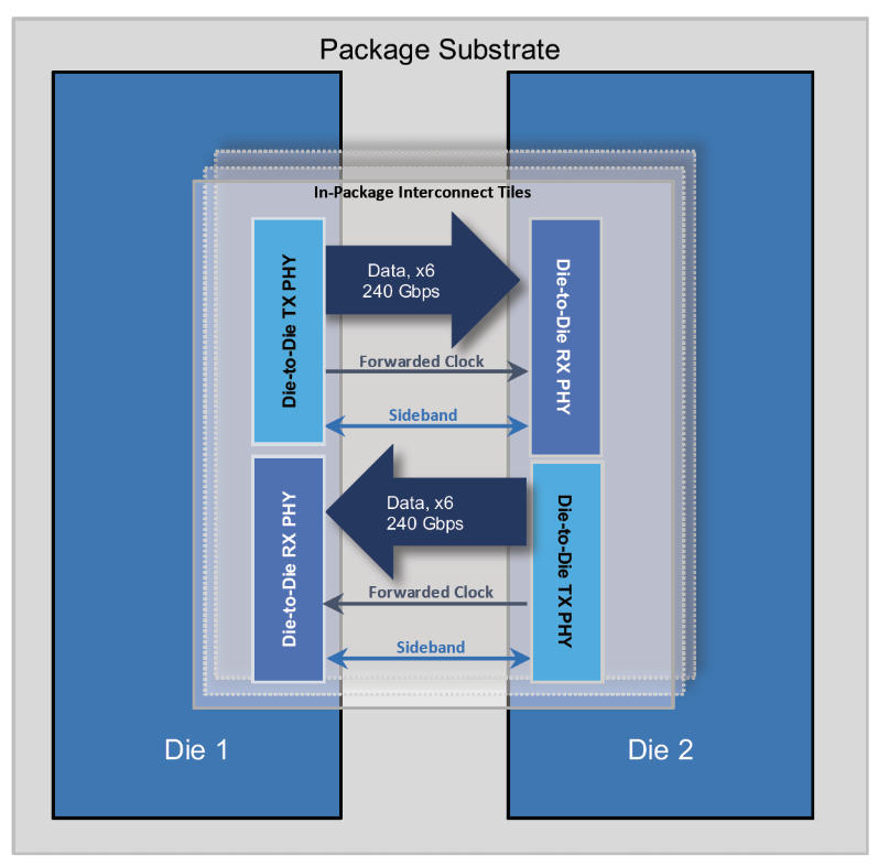
Cadence – UltraLink D2D
The Cadence UltraLink Die-to-Die (D2D) PHY enables SoC providers to deliver more customized solutions that offer higher performance and yields while also shortening development cycles and reducing costs through greater IP reuse. -
Cadence – Celsius
Control the thermal and stress impacts on your chiplets with Celsius Studio, the industry’s first unified AI-enabled multiphysics thermal platform that incorporates thermal, stress, and electronics cooling analysis. -
Cadence – HBM PHY
Cadence PHY IP for high-bandwidth memory (HBM) is supports high-performance 3D-stacked DRAM system-in-package (SiP) development. -
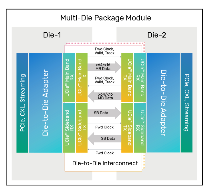
Cadence – UCIe PHY and Controller
The Cadence UCIe™ PHY is a high-bandwidth, low-power and low-latency die-to-die solution that enables multi-die system in package integration for high performance compute, AI/ML, 5G, automotive and networking applications. -
Ayar Labs In-Package Optical I/O Solution
The Ayar Labs optical I/O solution is a small-footprint, low-power, high-throughput alternative to copper backplane and pluggable optics-based interconnect solutions. Combining silicon photonics with standard CMOS manufacturing processes, Ayar Labs’ optical I/O solution delivers up to… -
-
Chiplet Data Exchange in XML Format (CDXML)
Chiplet Design Exchange (CDX) Workstream of ODSA focuses on electrical, mechanical, and thermal design exchange standards related to chiplets and integration in the context of multi chiplet modules, 2.5D and 3D Integrated Circuits (IC). This initial… -
-
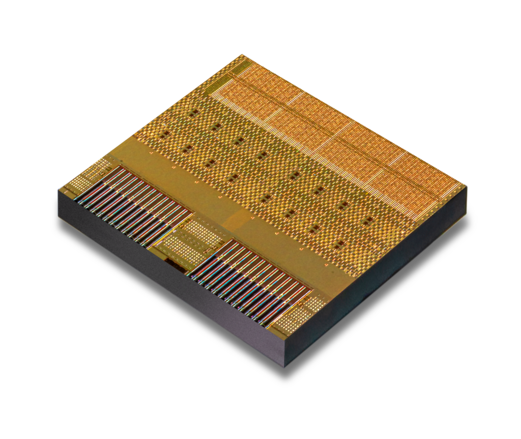
OpenHBI Specification
The ODSA OpenHBI or Open High Bandwidth Interface specification defines a high-performance die-todie or chiplet-to-chiplet interconnect on a medium such as a silicon interposer or equivalent technology in a common package. The OpenHBI defines an optimized…