
Chiplet architectures are redefining AI and HPC system design, making the co-optimization of logic, memory, and advanced packaging more critical than ever. Built on an advanced foundry logic base die, custom HBM (cHBM) offers greater architectural flexibility, enhanced computational capability, and improved energy efficiency for next-generation systems.
Advantages of integrating a foundry logic base die with HBM:
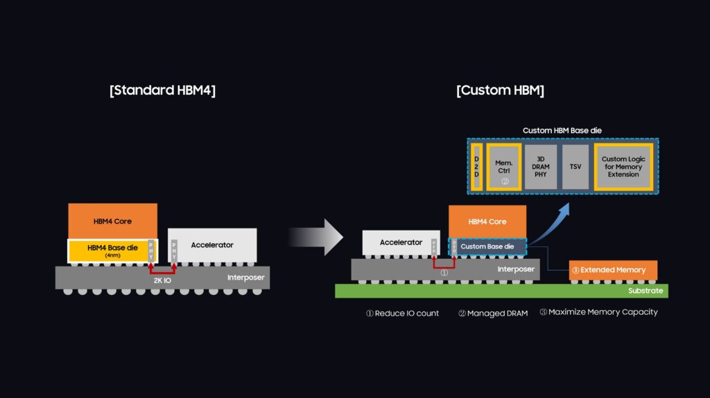
- Higher Bandwidth and Capacity: The foundry logic base die offers an optimized shoreline and utilizes high-speed a die-to-die (D2D) interfaces, increasing bandwidth and supporting additional HBM stacks compared to traditional HBM PHY-based implementations.
- Lower Latency and Power: Integrating the HBM controller into the base die streamlines data pathways, reducing power consumption and latency while simplifying system design.
- Advanced Logic Process Benefits: Implementing the base die on an advanced logic process improves power efficiency and enables higher-performance memory subsystem designs.
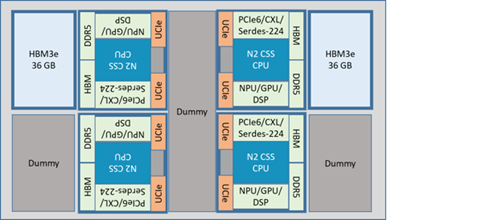
- Architectural Flexibility: A customized logic base die can integrate value-added functions — including accelerators, memory controllers, and CPUs — to create differentiated, workload-optimized chiplet architectures.
By combining advanced foundry logic processes with HBM, Samsung enables co-optimized chiplet architectures that deliver higher bandwidth, improved power efficiency, and greater design flexibility. This system-level approach helps customers build next-generation AI, HPC, and data-intensive computing platforms.